
Circuit Design and Physical Design for a Novel FPGA Architecture
| Led by: | Prof. Dr.-Ing. H. Blume, apl. Prof. Dr.-Ing. G. Payá Vayá |
| Team: | B. Bredthauer, C. Spindeldreier |
| Year: | 2013 |
| Funding: | Federal Ministry of Education and Reserach |
| Duration: | May 2013 - June 2014 |
| Is Finished: | yes |
Goal
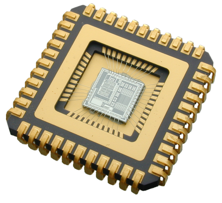
The BMBF funded FPGA-Project evaluates and analyses the implemtability and performance of a new type of field programmable gate array (FPGA) in the 28nm very large scale integration process technology.
The objective of this project is development and analysis of the integrated circuit and physical layout in 28nm technology of the new FPGA architecture, so far developed at Cologne Chip AG. Thereby the implementability of the reduction of chip area and energy consumption as well as the enhancement of timing, which have been shown by simulation, will be analyzed for the physical layout.
Contribution of IMS
The Architectures and Systems Group at the Institute of Microelectronic Systems will evaluate the new architecture in terms of chip area and energy consumption to current commercial and research FPGA architectures. Furthermore, a benchmarking based on common signal processing algorithms will be performed. The results will be used for the optimization and of the new FPGA architecture.
An evaluation of the existing custom place & route software will be done by the Electronic Design Automation Group of the Institute at the Microelectronic Systems. Several algorithmic enhancements of the existing place & route tool will be analyzed in order to increase the utilization of the proposed FPGA architecture and to decrease the timing paths;


